



Essential DFM Guidelines for Solder Paste Printing
A well-designed PCB doesn’t just function correctly—it must also be easy to manufacture consistently. That’s the goal of Design for Manufacturability (DFM). By considering manufacturing requirements during the PCB layout stage, engineers can reduce defects, shorten production time, and lower overall assembly costs.
One of the most critical manufacturing processes influenced by PCB layout is solder paste printing. Even with high-precision stencil printers, poor pad design or inadequate spacing can result in solder bridges, insufficient solder joints, tombstoning, and other assembly defects.
Optimizing your PCB layout before production helps ensure reliable solder paste deposition, resulting in higher yields and more dependable electronic assemblies.
What Is Design for Manufacturability (DFM)?
Design for Manufacturability is the practice of designing a PCB so it can be assembled efficiently, consistently, and with minimal defects. Rather than waiting until prototypes reveal manufacturing problems, DFM identifies potential issues during the design stage.
Benefits of DFM:
- Improves first-pass production yield
- Reduces assembly defects
- Lowers manufacturing costs
- Minimizes rework and scrap
- Accelerates time to market
- Improves long-term product reliability
Why Solder Paste Printing Is Critical
Solder paste printing is the first step in the SMT assembly process. A laser-cut stencil deposits carefully controlled amounts of solder paste onto each PCB pad before components are placed. Because every solder joint begins with the solder paste deposit, printing accuracy directly affects overall assembly quality.
Common Printing Defects
| Defect | Typical Cause | Potential Result |
|---|---|---|
| Solder bridging | Excess solder paste or pads too close together | Electrical shorts |
| Insufficient solder | Small apertures or paste loss | Weak or open joints |
| Tombstoning | Uneven solder volume or thermal imbalance | Lifted components |
| Component shift | Misaligned paste deposits | Placement defects |
| Voiding | Poor paste release or trapped gases | Reduced thermal performance |
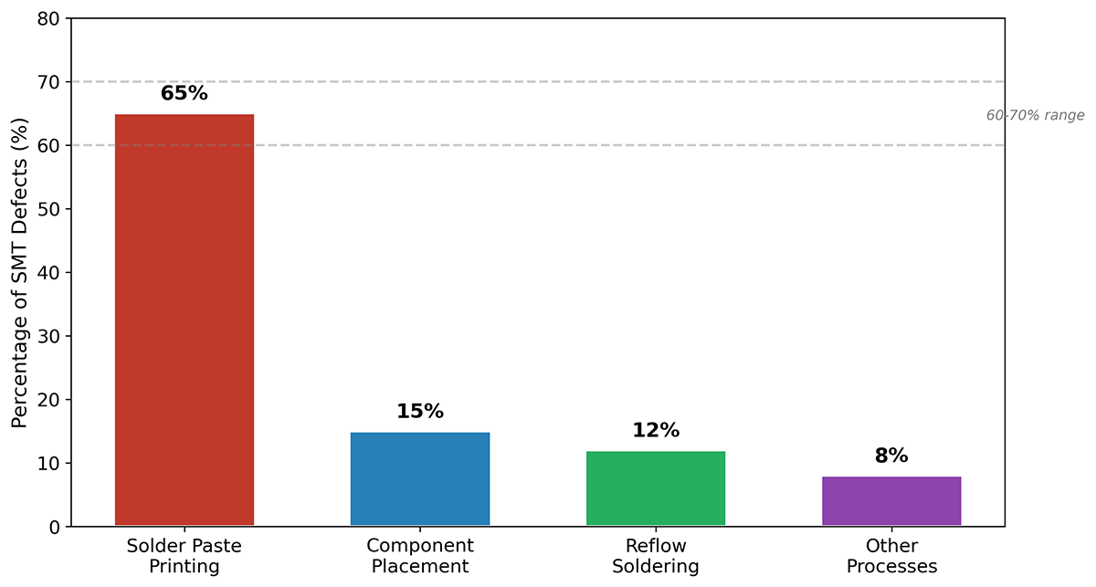
Sources of SMT Assembly Defects
Key PCB Layout Optimizations for Superior Solder Paste Printing
1. Master the Pad-to-Aperture Ratio
The solder paste stencil dictates where and how much paste is deposited onto the PCB pads. While stencil thickness is determined during manufacturing, your layout controls the copper pad dimensions.
- The Golden Rule: The stencil aperture (the opening) should generally match or be slightly smaller than the PCB pad (often a 1:1 ratio or a minor reduction of 10-20% in area).
- Aspect & Area Ratios: To ensure the solder paste actually releases from the stencil and sticks to the pad instead of staying clogged in the aperture, the Area Ratio (Area of Aperture Opening / Area of Aperture Wall) must be greater than 0.66. If your pads are too small or packed too tightly, the paste cannot cleanly transfer.
2. Perfect the Aspect Ratio for Fine-Pitch Components
As components get smaller (like 0201 or 01005 packages and fine-pitch BGAs), the window for error shrinks.
- Avoid placing heavy copper traces or large vias directly next to fine-pitch pads without adequate solder mask webbing.
- When designing for fine-pitch components, use rounded or square apertures with radiused corners rather than sharp rectangles. This shape optimization promotes a much smoother release of the solder paste from the stencil.
3. Implement Solder Mask Defined (SMD) vs. Non-Solder Mask Defined (NSMD) Pads Wisely
Choosing between SMD and NSMD pads drastically affects how paste spreads and prints:
- NSMD (Copper Defined): The solder mask opening is larger than the copper pad. This is preferred for most fine-pitch applications because it provides tighter copper tolerances and allows the solder paste to wrap around the sides of the pad, creating a stronger mechanical bond.
- SMD (Mask Defined): The solder mask overlaps the copper pad. This is excellent for larger components or areas prone to lifting, as the mask acts as an anchor. However, because mask registration can shift slightly, it can create uneven surfaces for solder paste printing if used incorrectly.
4. Conquer Thermal Sinking and Solder Thievery
Unbalanced heat distribution across a component can cause major printing and reflow headaches.
- The Tombstoning Effect: If one pad of a two-terminal component (like a resistor or capacitor) is connected to a massive ground plane and the other is connected to a thin trace, the side with the thin trace will heat up faster. The solder melts unevenly, causing the component to stand up on one end—a defect known as tombstoning.
- Thermal Reliefs: Always use thermal relief connections when pads link to large copper planes. This ensures even heating and prevents the ground plane from acting as a giant heat sink that disrupts the paste reflow.
5. Prevent Solder Migration with Via-in-Pad Management
Placing a via directly on a component pad (Via-in-Pad) is a great way to save space in high-density designs, but it poses a massive risk to solder paste printing.
- If an open via sits on a pad, the solder paste will liquefy during reflow and wick down into the hole, leaving an insufficient amount of solder on the pad to secure the component.
- The Fix: If you must use Via-in-Pad, ensure the vias are capped, filled, and planarized (filled with epoxy and plated over with copper) during PCB fabrication. If budget doesn’t allow for filled vias, move the vias outside the pad and seal them with solder mask to create a barrier.
6. Incorporate Clear Fiducial Marks
Modern solder paste printers use advanced optical systems to align the stencil perfectly with the PCB. They can’t do this without high-quality fiducial marks.
- Place at least three global fiducial marks on the corners of your PCB panel.
- Keep a clear keep-out zone (free of traces, mask, and silkscreen) around the fiducials so the printer’s vision system can easily recognize them.
Stencil Considerations That Complement Your Layout
While the focus is on PCB layout, remember these interact closely with stencil design:
- Aperture size: Often 5–10% smaller than pads for standard components; adjust for fine-pitch.
- Aspect and Area Ratios: Aim for Area Ratio > 0.66 and Aspect Ratio > 1.5 for reliable paste release.
- Stencil thickness: Typically 0.1–0.15 mm; match to your smallest component requirements.
How EMS, Inc. Supports Design for Manufacturability
At EMS, Inc., manufacturability is evaluated before production begins. Our engineering team reviews PCB layouts to identify opportunities for improving solder paste printing, SMT assembly, and overall manufacturing efficiency.
Our Design for Manufacturability review includes:
- PCB footprint verification
- Component spacing evaluation
- Solder paste printing optimization
- Stencil design recommendations
- Thermal management review
- Panelization guidance
- Assembly process recommendations
By identifying potential manufacturing issues early, we help customers reduce defects, improve yields, and move from prototype to production with greater confidence.