
Let Us Know How We Can Help. We Are Your Dedicated Solutions Provider.
Cavity-Mounted Sensor
- Home
- electronics-manufacturing-services-projects
- Transportation & Logistics
- Cavity-Mounted Sensor
Case Study: Precision Assembly of a Cavity-Mounted Sensor Using Advanced Solder Paste Jetting Technology
Published: December 10, 2021, Category: Transportation & Logistics
Overview
A customer approached EMS with a PCB design that included a recessed cavity intended to house a fine-pitch, bottom-terminated sensor device. While electrically and mechanically beneficial, the cavity introduced significant manufacturing challenges—particularly in the application of solder paste and accurate component placement. Traditional SMT production methods were not capable of reliably supporting the design.
EMS leveraged its advanced solder paste jetting system and engineering expertise to deliver a high-quality, repeatable assembly process that met the customer’s requirements and enabled the success of the product.
THE cHALLENGE
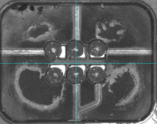
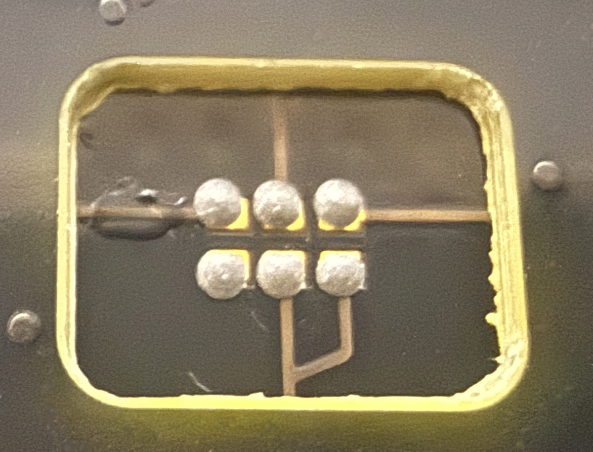
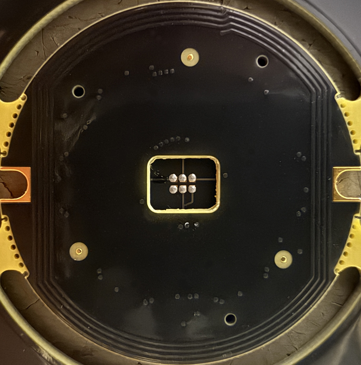
1. Recessed PCB Cavity
The PCB included a pocket machined into its thickness to partially recess a sensitive sensor component.
This geometry created a fundamental obstacle:
- Traditional stencil printing cannot reach pads inside a recessed cavity.
- Attempting to modify the stencil would risk insufficient paste volume, paste smearing, or damage to the stencil.
Why this matters?
Stencil printing works only when the paste can be deposited on a flat, unobstructed surface. Even slight step-downs can result in poor gasketing and print defects. A deep cavity makes stencil printing impossible.
2. Fine-Pitch, Bottom-Terminated Device
The component intended to sit inside the cavity featured:
- A bottom-terminated land pattern
- Very fine-pitch pads
- Tight tolerances for paste volume and alignment
This type of component requires highly controlled solder deposition to ensure:
- Proper wetting
- Avoidance of voids
- Reliable mechanical and thermal performance
Solution
1. Advanced Solder Paste Jetting Technology
To overcome the cavity constraint, EMS deployed its high-precision solder paste jetting system.
Unlike stencil printing – which applies solder paste by squeegeeing material through laser-cut apertures – jetting dispenses paste drop-by-drop through a precision valve system, allowing three-dimensional control.
How jetting solved the problem?
- Directly deposited paste into the recessed cavity without requiring a modified stencil
- Controlled volume and dot placement ensured consistent paste deposits even on extremely fine-pitch pads
- Eliminated the need for specialized tooling or redesign of the PCB
- Enabled paste shaping and distribution that optimized reflow performance for a bottom-terminated package
This capability allowed EMS to create a reliable process where traditional solder application methods would fail.
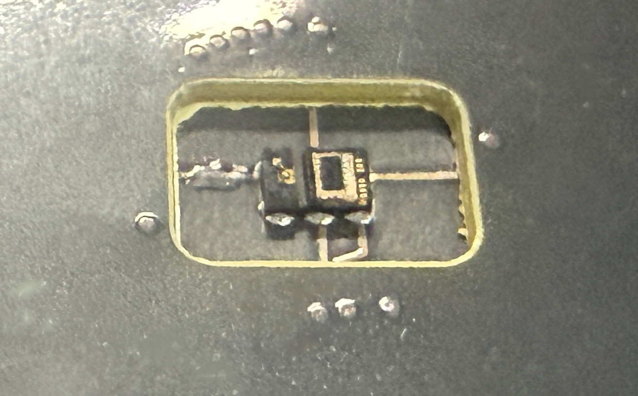
2. Precision Pick-and-Place in a Cavity
Once paste was applied via jetting:
- EMS programmed its placement system to accurately position the sensor device into the recessed pocket
- Specialized fiducials and vision routines were used to compensate for depth and shadows
- The placement nozzle and force parameters were tuned to ensure proper seating within the cavity without damaging the component
Results
- Successfully assembled a design that cannot be built using standard SMT processes – The combination of cavity geometry and fine-pitch pads would have made the board incompatible with traditional PCB assembly lines.
- No PCB design changes required – EMS delivered a manufacturable solution without altering the customer’s electrical or mechanical design intent.
- High yield and repeatability – Jetting allowed precise paste control, dramatically reducing the risk of opens, voids, or insufficient solder on fine-pitch bottom-terminated pads.
- Enabled true 3D design freedom – By using solder paste jetting, the customer was able to leverage depth as a design parameter, unlocking possibilities not feasible with standard 2D planar SMT rules.
Conclusion
This project demonstrates EMS’s ability to solve unique, highly technical assembly challenges through a combination of engineering expertise and advanced manufacturing technology.
By incorporating solder paste jetting—a process still uncommon in many contract manufacturing environments—EMS enabled a breakthrough design that would otherwise be impractical or impossible to assemble using traditional PCB manufacturing techniques.